Loop Antenna - SPI Read and Write
Now that I have confirmed the stepper driver is working properly, I want to establish SPI communication for configuration and status readback. This will be especially important to enable the stall detection feature I am using for homing.
First, I wrote a function to read and write the registers on the TMC2130 using SPI. This is a read/write function – the only difference is that in a 'write' operation the address of the register is OR'd with 0x80.
tmc_readwrite_register():
uint32_t tmc_readwrite_register(uint8_t addr,
    uint32_t data, uint8_t set_write_flag)
{

    uint8_t rx_data[5];
    uint8_t tx_data[5];
    uint32_t payload =0;
    uint8_t send_count = 2;

    if(set_write_flag) {
        addr |= 0x80;
        send_count = 1;
    }

    //send twice on receive according to TMC2130 datasheet
    for (uint8_t i = 0; i < send_count; i++) {

        tx_data[0] = addr;
        tx_data[1] = (data >> 24) & 0x00ff;
        tx_data[2] = (data >> 16) & 0x00ff;
        tx_data[3] = (data >> 8)  & 0x00ff;
        tx_data[4] = (data)	      & 0x00ff;

        while(HAL_SPI_GetState(&hspi1) != HAL_SPI_STATE_READY);
        HAL_GPIO_WritePin(MOTOR_CS_GPIO_Port,
            MOTOR_CS_Pin, GPIO_PIN_RESET);

        while(HAL_SPI_GetState(&hspi1) != HAL_SPI_STATE_READY);
        HAL_SPI_TransmitReceive(&hspi1, (uint8_t *) tx_data,
            (uint8_t *) rx_data, sizeof(rx_data), HAL_MAX_DELAY );

        while(HAL_SPI_GetState(&hspi1) != HAL_SPI_STATE_READY);
        HAL_GPIO_WritePin(MOTOR_CS_GPIO_Port, MOTOR_CS_Pin, GPIO_PIN_SET);

    }

    payload = (rx_data[1] << 24) + (rx_data[2] << 16)
            + (rx_data[3] << 8 ) +  rx_data[4];


    return payload;

}
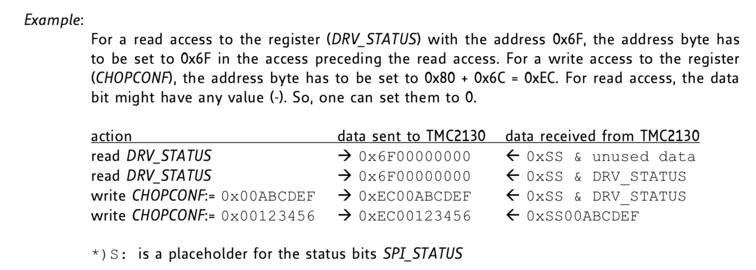
The read commands are sent twice in a row. This is because the TMC2130 delays the response by one SPI transaction. This section of the datasheet explains it:
It may be possible to optimize some read operations by creating an interface to pipeline multiple commands in a row. Its also possible to take advantage of multiple subsequent reads from the same register. I don't think either of those will be necessary and for now I am accepting that I occasionally send a redundant command.
In the main loop, after initializing SPI and GPIO blocks, I put the following code into a repeating loop:
data = tmc_readwrite_register(TMC_REG_IOIN, 0, 0);
TMC_REG_IOIN is defined as the 8-bit address of the IOIN register. This register contains the logic level of all of the IO pins on the TMC2130. It also has a few bits which always read back '1', which will be useful for testing the SPI interface.
I attached my Saleae logic analyzer and it looks like communication is generally working.
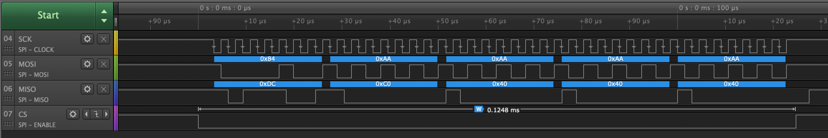
If I change the command to:
data = tmc_readwrite_register(TMC_REG_IOIN, 0xAAAAAAAA, 1);
the MOSI signal changes accordingly:

While MOSI looks good, the MISO line doesn't look correct.The value I read is inconsistent with the datasheet description for the IOIN register. Comparing the timing diagram in the TMC2130 datasheet to the logic analyzer waveforms shows that the wrong clock edge is being used. I changed changed the line in spi.c to select the 2nd clock edge:
hspi1.Init.CLKPhase = SPI_PHASE_2EDGE;
After this, the SPI interface is working well in both directions.
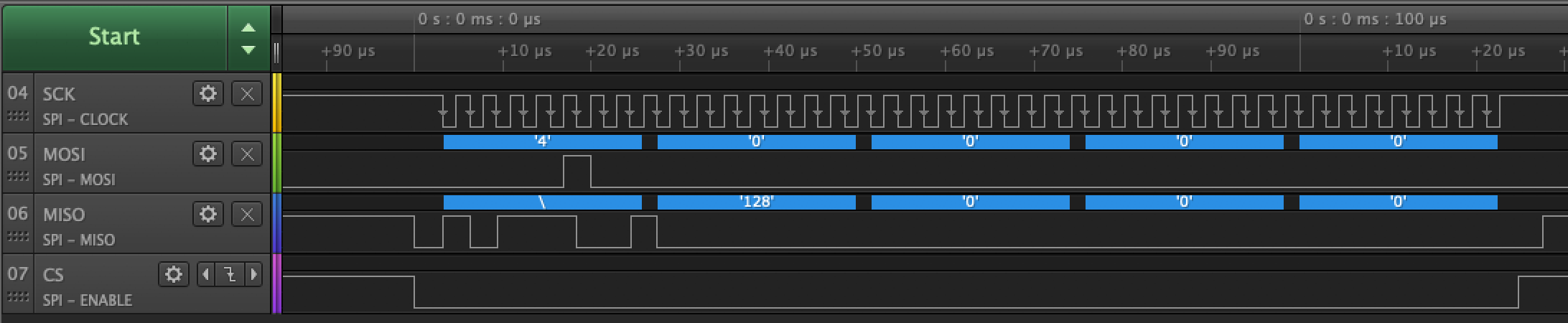
Here is an example of reading the IOIN register with the "DIR" pin set to 3v3:
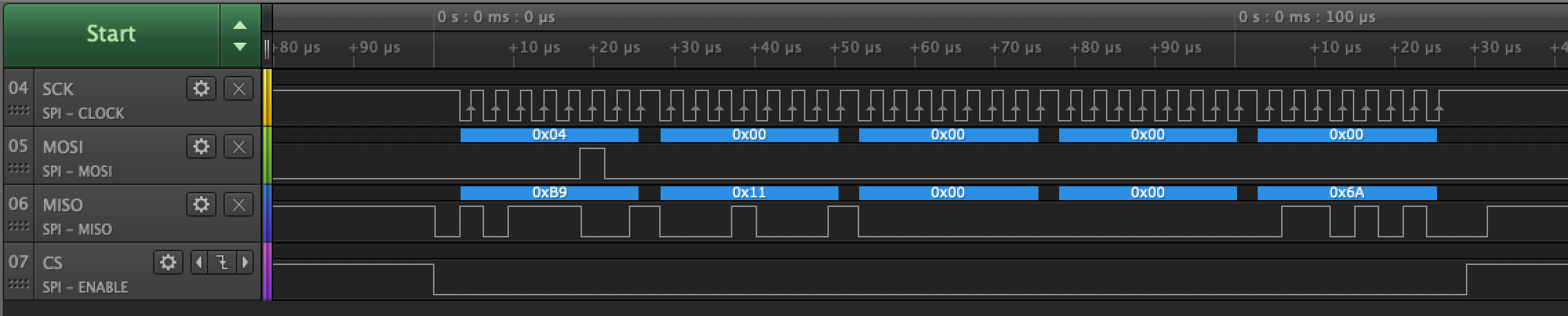
And here is the same trace with the "DIR" pin connected to GND:
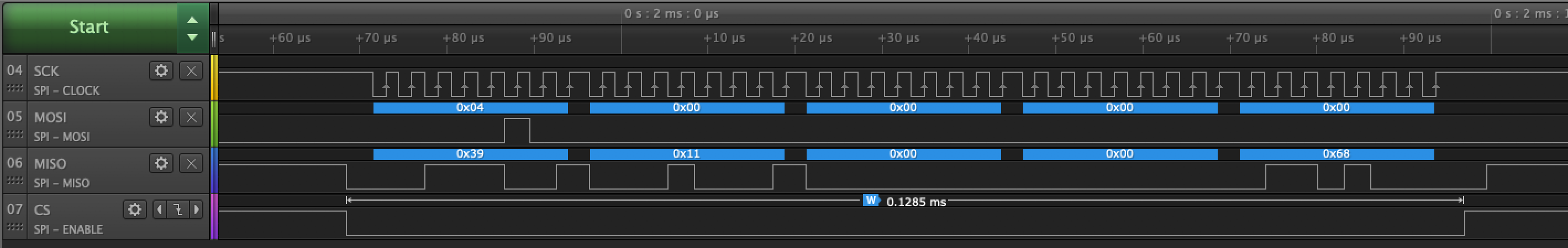
As expected, bit 1 switches from a 1 to a zero and the rest of the input data remains unchanged:
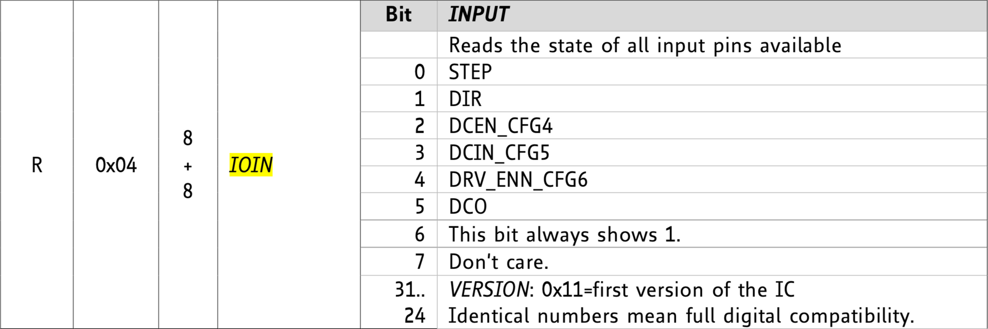
Also note that bits 24-31 are 0x11, as indicated in the datasheet.
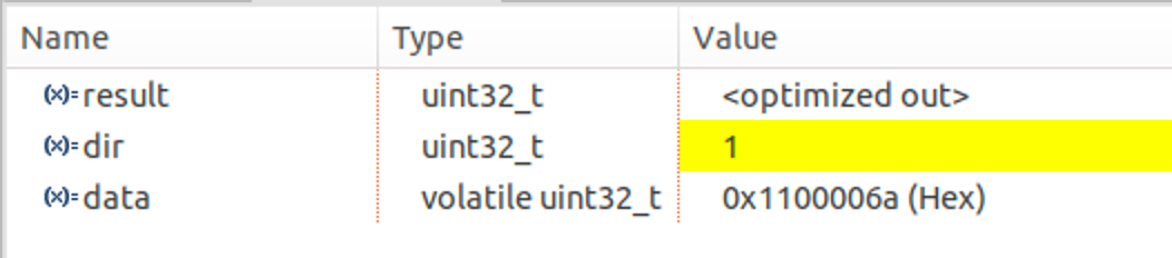
I am also seeing the correct data returned when I check the value in the debugger:
Now I need to find the correct initialization values for the TMC2130 stepper and write an initialization function.